HL5616
Patent No.:
- US 7,023,221 B1 (U.S.A.)
- I 259908 (R.O.C.)
- EP 1791260 B1 (EUROPE)
- ZL 200510080231.9 (CHINA)
- 特許第4365817号 (JAPAN)
- US 7,944,217 B2 (U.S.A.)
GENERAL DESCRIPTION
HL5616 is a multi-keys capacitive touch sensor IC with very high noise rejection capability. The circuit is designed to be applied in home appliance products, where the EMI interference can be very strong. In the application field of the home appliance products, Triac is often used as the driver of the load. In order to reduce the driving current consumption of the Triac, a zero crossing circuit is designed in the HL5616, and the pulse-mode trigger current can be provided in HL5616.
The sensors of the capacitive touch sensor IC are composed of multiple arrays of sensor plates. In HL5616 16 touch sensor plates are provided.
HL5616 can communicate with external microprocessor through SCL and SDA pins. When a key is touched the READYN pin is activated to LOW state, and which means DATA is ready to be read. SDA and SCL are serial data bus.
HL5616 is fabricated by CMOS process with very low power consumption. In order to expand the number of the keys multiple numbers of HL5616 can be used in one system. The maximum number of HL5616 can be used in one system is eight. There are address pins ADD2, ADD1 and ADD0 which can be used to identify which HL5616 is chosen by microprocessor.
FEATURES
- Mixed mode integrated circuit
- Low operating current
- Serial digital data bus
- Parameters can be programmed by external microprocessor
- Keys of keypad are expandable
- Built-in regulator circuit
- Three address pins which can be used to identify HL5616
- Built-in DATA buffer
- High temperature variation resistance
- High noise interference resistance
- Pulse mode of Triac trigger current is provided
ELECTRICAL CHARACTERISTICS (VDD=4.5V, GND=0V, MODE1=0, VSL=1, Ta=+25℃)
PARAMETER |
CONDITIONS |
MIN |
TYP |
MAX |
UNITS |
| VDD | Supply Voltage | 3.5 | 4.5 | 6.0 | V |
| Standby Current | MRSTN = GND | 0.2 | uA | ||
| Operating Current | fosc=1MHz | 0.5 | mA | ||
| Input low voltage | 0.9 | V | |||
| Input high voltage | 3.5 | V | |||
| Output low voltage | I out = 15mA | 0.2 | 0.4 | V | |
| Output high voltage | I out = 5mA | 4.0 | 4.3 | V |
ELECTRICAL CHARACTERISTICS (VDD=3.3V, GND=0V, MODE=1, VSL=1, Ta=+25℃)
| PARAMETER | CONDITIONS | MIN | TYP | MAX | UNITS |
| VDD | Supply Voltage | 3.1 | 3.3 | 3.5 | V |
| Standby Current | MRSTN = GND | 0.2 | uA | ||
| Operating Current | fosc=1MHz | 0.5 | mA | ||
| Input low voltage | 0.9 | V | |||
| Input high voltage | 2.4 | V | |||
| Output low voltage | I out = 15mA | 0.2 | 0.4 | V | |
| Output high voltage | I out = 5mA | 2.6 | 3.1 | V |
ELECTRICAL CHARACTERISTICS (VDD=3V, GND=0V, MODE=1, VSL=0, Ta=+25℃)
PARAMETER |
CONDITIONS |
MIN |
TYP |
MAX |
UNITS |
| VDD | Supply Voltage | 2.7 | 3.0 | 3.5 | V |
| Standby Current | MRSTN = GND | 0.2 | uA | ||
| Operating Current | fosc=1MHz | 0.4 | mA | ||
| Input low voltage | 0.9 | V | |||
| Input high voltage | 2.1 | V | |||
| Output low voltage | I out = 10mA | 0.2 | 0.4 | V | |
| Output high voltage | I out = 3mA | 2.4 | 2.8 | V |
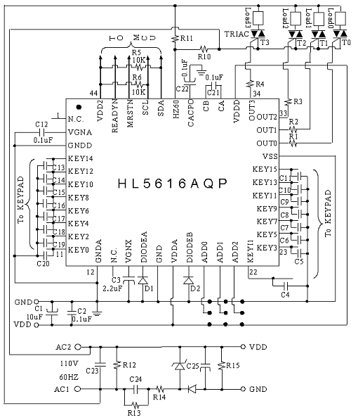
APPLICATION CIRCUIT For AC