HL5516
GENERAL DESCRIPTION
HL5516 is a multiple point object proximity sensor IC, which can be used to determine the position of an object in a keypad and can be called capacitive touch sensor.
The sensors of the object position detector are composed of multiple arrays of sensor plates. HL5516 offers 16 touch keys.
HL5516 can communicate with external microprocessor through SCL and SDA pins. When a key is touched the READYN pin is activated to LOW state, and which means DATA is ready to be read. SDA and SCL are serial data bus.
HL5516 is fabricated by CMOS process with very low power consumption. There are two operating mode, low power current mode and normal mode. In low power mode, the operating current is only about 7uA (LST1=1 LST0=1). In normal operating mode, the response time is very fast. All of the 16 keys can operate in the low power state. When there is a key detected, HL5516 will enter into normal state with fast response time. In the normal state, HL5516 will enter into low power state if there is not key detected for a period of time.
In order to expand the number of the keys multiple numbers of HL5516 can be used in one system. The maximum number of HL5516 can be used in one system is eight. There are address pins ADD2, ADD1 and ADD0 which can be used to identify which HL5516 is chosen by a microprocessor.
FEATURES
- Mixed mode integrated circuit
- Low operating current
- Serial digital data bus
- Dual operating modes: low power mode and normal mode
- Extra low current in low power mode (7uA:LST1=1 LST0=1)
- Parameters can be programmed by external microprocessor
- Keys of keypad are expandable
- Built-in regulator circuit
- Three address pins which can be used to identify HL5516
- High temperature variation resistance
- High noise rejection
ABSOLUTE MAXIMUM RATING
Supply Voltage (VDD to GND) --------------------------- 5.5VInput Voltage Range -------------------------------- (GND - 0.3V) to (VDD + 0.3V)
Operating Temperature Range ------------------------- -40℃ to +80℃
ELECTRICAL CHARACTERISTICS
(VDD=4.5, GND=0V, VSL=1, Ta=+25℃)
PARAMETER |
CONDITIONS |
MIN |
TYP |
MAX |
UNITS |
| VDD | Supply Voltage | 3.5 | 4.5 | 5.5 | V |
| Standby Current | ENB = GND | 0.2 | uA | ||
| Operating Current | Normal State | 95 | uA | ||
| Low Power State (LST1=1 LST0=1) | 12 | uA | |||
| Oscillation frequency | 1 | MHz | |||
| Input low voltage | 0.9 | V | |||
| Input high voltage | 3.5 | V | |||
| Output low voltage | I out = 15mA | 0.2 | 0.4 | V | |
| Output high voltage | I out = 5mA | 4.0 | 4.3 | V |
ELECTRICAL CHARACTERISTICS
(VDD=3V, GND=0V, VSL=0, Ta=+25℃)PARAMETER |
CONDITIONS |
MIN |
TYP |
MAX |
UNITS |
| VDD | Supply Voltage | 2.5 | 3.0 | 5.5 | V |
| Standby Current | ENB = GND | 0.2 | uA | ||
| Operating Current | Normal State | 75 | mA | ||
| Low Power State (LST1=1 LST0=1) | 7 | uA | |||
| Oscillation frequency | 1 | MHz | |||
| Input low voltage | 0.9 | V | |||
| Input high voltage | 2.1 | V | |||
| Output low voltage | I out = 10mA | 0.2 | 0.4 | V | |
| Output high voltage | I out = 3mA | 2.4 | 2.8 | V |
Note: Low power state current depends by key number, LST1 and LST0
OPERATION OF THE SYSTEM
HL5516 is programmed for serial interface with micro-controller. The instruction data is transferred via a pair of serial data and clock input pins. Data is input from SDA and SCL pins.
Before the operation of the system, a low pulse must be send to the ENB pin. The parameters of HL5516 must be set in 64ms after the ENB pin set High level.
The parameters include:
1. DB5, DB4, DB3, DB2, DB1, DB0,
2. FREQ, DA5, DA4, DA3, DA2, DA1, DA0
2. TB, TA, T1, T0, LT2, LT1, LT0, LOPWR,
3. REFADJ, REFD, LST1, LST0, R1, R0, DCK1, DCK0
There are two sets of sensitivity setting in the HL5516. The DB5~DB0 define the sensitivity that Key state change from ON to OFF. The DA5~DA0 define the sensitivity that Key state change from OFF to ON.
The value setting 000001 is the most sensitive level and 111111 is the least sensitive level.
The value of DA5~DA0 is bigger than the value of DB5~DB0.
FREQ defines the operating frequency of the system. If FREQ=0, the output of the oscillator is sent to the system directly. If FREQ=1, the output of the system clock is divided by 2 before sent to the system.
TB TA, T1 T0 and REFD determine the time period for each key waiting for a stable state.
REFD=0

REFD=1

LT2 LT1 and LT0 define the time to enter low power mode if no key ON.

LOPWR define the operating mode. If LOPWR=0, the operating mode will always stay in normal mode. If LOPWR=1, there have two operating mode, low power current mode and normal mode.
REFADJ =0, the output of key will stay active for a period of time. REFADJ =1, is used in long-time level-hold.
LST1 and LST0 define sampling time in low power mode.

R1, R0 defines the number of keys in a keypad. The relation between R1, R0 and key number is:

DCK1, DCK0 define the times that the system will check status of the key to determine that key is touched. If DCK1, DCK0 set 1X, the systems will response slower.

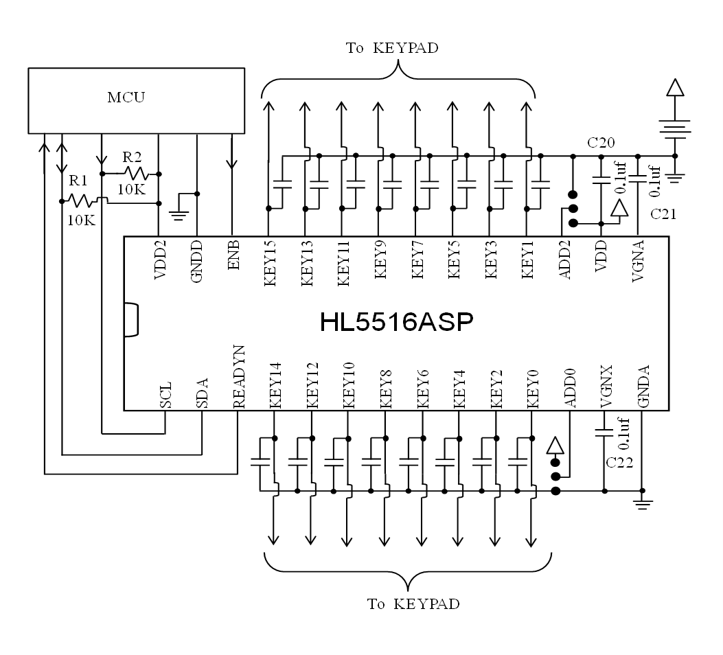
APPLICATION CIRCUIT
(SSOP 28PIN)