GENERAL DESCRIPTION
The HL8042A Heart Pulse Detector is a single chip AC type photo-sensing heart pulse detection system with the environmental light cancellation function. With a power supply booster and a built-in power regulator, HL8042A has wide operating voltage range and high immunity to power noise induced by other devices. HL8042A receives and amplifies the heart pulse signal from external photo sensor with a few external components. The LED driver of HL8042A outputs a 600Hz high pulse signal with 1/16 duty, so that the average LED driving current is only 1/16 of peak driving current and the power consumption is largely reduced. The high output voltage of LED driver can drive high efficient green LED and make HL8042A applied suitably in the system of using a reflect type photo sensor.
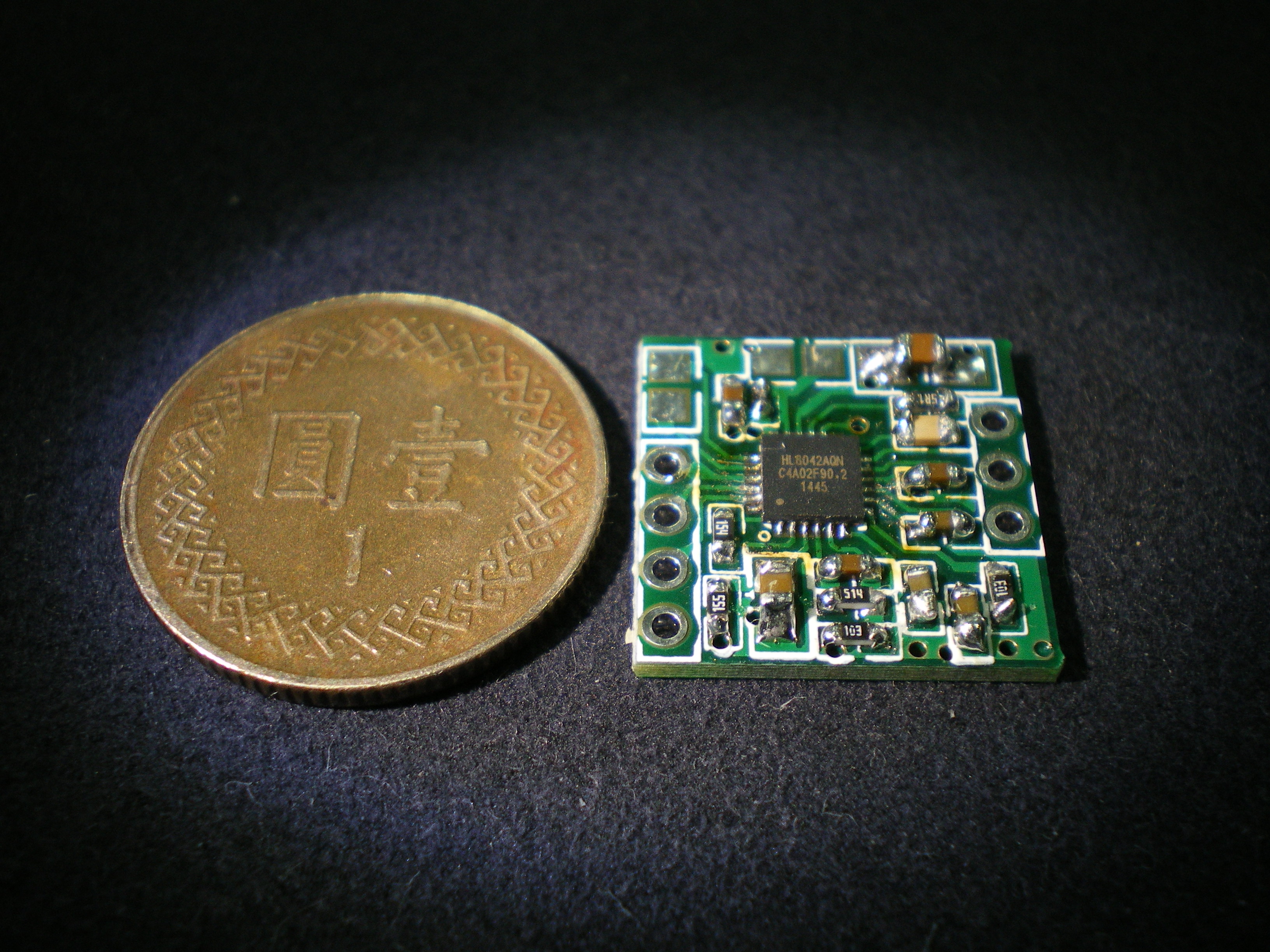
Demostration
FEATURES
- Wide operating voltage range (2.4V to 5V)
- Built-in power supply booster
- Built-in power regulator
- AC type photo-sensing heart pulse detection
- Environmental light cancellation
- 1/16 duty LED driving pulse
- High LED driver output voltage
- Low power consumption
ABSOLUTE MAXIMUM RATING
Supply Voltage (VDD to VSS) --------------------------------------------- 6V
Input Voltage Range ------------------------- (VSS - 0.3V) to (VDD + 0.3V)
Operating Temperature Range --------------------------------- 0℃ to +60℃
ELECTRICAL CHARACTERISTICS (VDD=3V, GND=0V, Ta=+25℃)
PARAMETER |
CONDITIONS |
MIN |
TYP |
MAX |
UNITS |
Standby Current |
ENB = 0V |
|
|
10 |
uA |
Operating Current |
ENB = 3V |
|
5 |
|
mA |
Operating Voltage |
Figure 1 |
|
|
3.3 |
V |
ENB input low voltage |
|
|
|
0.8 |
V |
ENB input high voltage |
|
2.2 |
|
|
V |
PULSE output low voltage |
Iout = -0.1mA , |
|
|
0.5 |
V |
PULSE output high voltage |
Iout = 0.1mA , |
2.5 |
|
|
V |
EMIT output current |
EMIT = 2.2V |
20 |
|
|
mA |
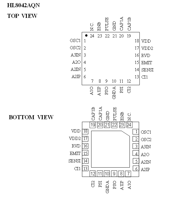
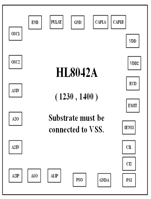
PIN DESCRIPTION
PIN NAME |
FUNCTION |
OSC1 |
Input of oscillator |
OSC2 |
Output of oscillator |
A3IN |
Negative input of third amplifier |
A2O |
Output of second amplifier |
A2IN |
Negative input of second amplifier |
A2IP |
Positive input of second amplifier |
A1O |
Output of first amplifier |
A1IP |
Positive input of first amplifier |
PSO |
Output of pulse sample |
PSI |
Input of pulse sample |
CI2 |
Output of photo sensor current integrator |
CI1 |
Input of photo sensor current integrator |
SENSI |
Photo sensor input |
EMIT |
Photo emitter driver |
RVD |
Regulated positive power supply output |
VDD2 |
Positive output of power supply booster |
VDD |
Positive input of power supply |
CAP1B |
First output of power supply booster |
CAP1A |
Second output of power supply booster |
GND |
Negative input of power supply |
PULSE |
Heart pulse signal output |
ENB |
Chip enable input , high active |
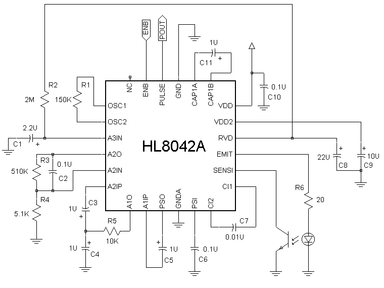
TYPICAL APPLICATION CIRCUIT 1
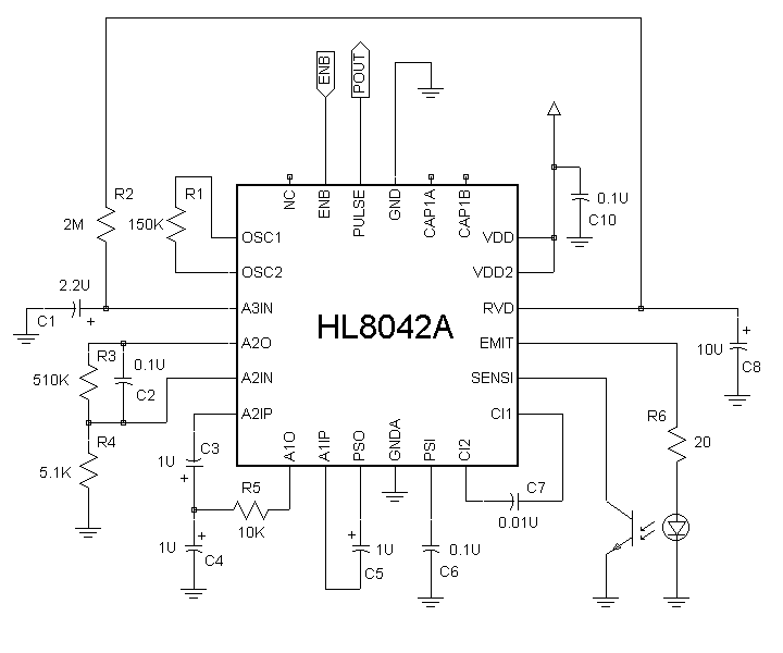
TYPICAL APPLICATION CIRCUIT 2
BODING PAD DIAGRAM
BODING PAD DIAGRAM (cont.)
PAD NO. |
NAME |
X |
Y |
PAD NO. |
NAME |
X |
Y |
1 |
OSC1 |
150 |
1220 |
13 |
CI1 |
1050 |
350 |
2 |
OSC2 |
150 |
1010 |
14 |
SENSI |
1050 |
490 |
3 |
A3IN |
150 |
800 |
15 |
EMIT |
1080 |
640 |
4 |
A2O |
150 |
600 |
16 |
RVD |
1080 |
810 |
5 |
A2IN |
150 |
390 |
17 |
VDD2 |
1110 |
960 |
6 |
A2IP |
150 |
180 |
18 |
VDD |
1080 |
1140 |
7 |
A1O |
290 |
180 |
19 |
CAP1B |
980 |
1280 |
8 |
A1IP |
430 |
180 |
20 |
CAP1A |
870 |
1280 |
9 |
PSO |
600 |
150 |
21 |
GND |
690 |
1280 |
10 |
GNDA |
830 |
150 |
22 |
PULSE |
520 |
1280 |
11 |
PSI |
1050 |
150 |
23 |
ENB |
310 |
1280 |
12 |
CI2 |
1050 |
250 |
|
|
|
|
PIN CONNECTION DIAGRAM QFN 24PIN