GENERAL DESCRIPTION
HL8030 is a mixed mode integrated circuit used to measure the impedance of an object. The sensor is formed by four probes which can be composes of two pairs metal plates. By contact with an object the impedance between the probes can be measured. The circuit composes of analog circuit, digital circuit and digital signal processor. Besides to measure the impedance, the noise caused by RF interference can be eliminated by the system. The output of the system consists of two pins, DATA and CLOCK. The output format is a synchronous data output which consists of 11 data bits, an error bit and an over-range bit. By built-in open circuit detector, there is not data output when circuit is open loop. There is an input pin to enable the system, and the standby current is zero in disable state. There are two measurement ranges, standard and programmable. In standard mode the parameters is set in the IC. In programmable mode, the parameters must input from IC input pin.
FEATURES
- Two operating voltage selectable
- Low operating current
- High precision and stable output
- Minimum external components and only two precision components
- Output data including error and over-range bits
- Programmable measurement range
ABSOLUTE MAXIMUM RATING
- Supply Voltage (VDD to VGN) --------------------- 5.5V
- Input Voltage Range --------------------------------- (GND - 0.3V) to (VDD + 0.3V)
- Operating Temperature Range------------------------ 0℃ to +60℃
ELECTRICAL CHARACTERISTICS (VDD=4.5V, GND=0V, Ta=+25℃)
ELECTRICAL CHARACTERISTICS (VDD=3V, GND=0V, Ta=+25℃)
PARAMETER |
CONDITIONS |
MIN |
TYP |
MAX |
UNITS |
| VDD | Supply Voltage | 2.5 | 3.0 | 3.6 | V |
| Standby Current | ENBN=0V or CLOCKI=0V | 0.1 | uA | ||
| Operating Current | fosc=500kHz | 4 | mA | ||
| Oscillation frequency | 500 | kHz | |||
| Frequency stability | Test at VDD=3V and 2.5V | 0.01 | % | ||
| Input low voltage | 0.8 | V | |||
| Input high voltage | 2.4 | V | |||
| Output low voltage | 0.8 | V | |||
| Output high voltage | 2.4 | V |
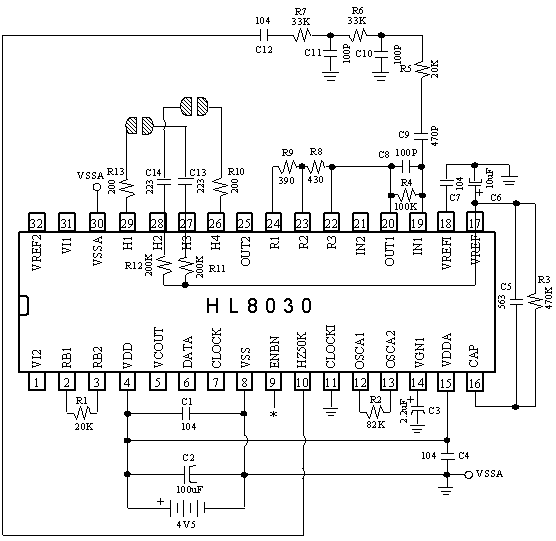
PIN DESCRIPTION
| PIN NO. | PIN NAME | I/O | FUNCTIONAL DESCRIPTION |
| 1 | VI2 | OUT | Output pin to hand pulse meter input |
| 2 | RB1 | I/O | Resistor used to set the current in analog circuit |
| 3 | RB2 | I/O | Resistor used to set the current in analog circuit |
| 4 | VDD | Positive power supply of digital circuit | |
| 5 | NC | No connection | |
| 6 | DATA | OUT | Output to transfer data to external CPU |
| 7 | CLOCK | OUT | Clock used to strobe data to external CPU |
| 8 | VSS | Negative power supply of digital circuit | |
| 9 | ENBN | IN | Input pin to enable HL8030, ENBN=0 chip is enable. ENBN=1 chip is disable. |
| 10 | HZ50K | OUT | 50kHz output wave when fosc=500kHz |
| 11 | CLOCKI | IN | Input pin used to set parameters in HL8030 and to choose the mode |
| 12 | OSCA1 | IN | Oscillator input pin |
| 13 | OSCA2 | OUT | Oscillator output pin |
| 14 | VGN1 | OUT | Power supply regulator |
| 15 | VDDA | Positive power supply for analog circuit | |
| 16 | CAP | OUT | Capacitor connection pin |
| 17 | VREF | OUT | Reference voltage output |
| 18 | VREFI | IN | Reference voltage input |
| 19 | IN1 | IN | Inverting input of the first amplifier |
| 20 | OUT1 | OUT | Output of the first amplifier |
| 21 | IN2 | IN | Inverting input of the second amplifier |
| 22 | R3 | IN | Resistor connection pin |
| 23 | R2 | IN | Resistor connection pin |
| 24 | R1 | IN | Resistor connection pin |
| 25 | OUT2 | OUT | Output of the second amplifier |
| 26 | H4 | IN | Sensor input pin |
| 27 | H3 | IN | Sensor input pin |
| 28 | H2 | IN | Sensor input pin |
| 29 | H1 | IN | Sensor input pin |
| 30 | VSSA | Negative power supply for analog circuit | |
| 31 | VI1 | OUT | Output pin to hand pulse meter input |
| 32 | VREF2 | OUT | Common terminal of hand pulse meter |
Application circuit