Patent No.
- US 7,565,470 B2 (U.S.A.)
- I 321734 (R.O.C.)
- ZL 2008 1 0161361.9 (CHINA)
GENERAL DESCRIPTION
HL5225 is a 3 channel LED driver with 6 bits device address identifier. There are 3 independent 4 bits LED current controllers. A common 8 bits PWM brightness controller is used to control the 3 LED drivers simultaneously. A serial data input port is used to receive control data for LED driver, and a serial data output port provides cascade serial data transformation.
FEATURES
- 3 channel LED driver
- 6 bits device address
- 3 4-bits LED current controllers
- 8 bits PWM brightness controller
- Serial data input and output ports
APPLICATION
- LED Light Bar
- LED Light Strip
- LED Light String
- LED Moving Sign
- LED Decoration Lamp
- Christmas LED Light
ABSOLUTE MAXIMUM RATING
- Power Supply -------------------------- 5V
- Input Voltage -------------------------- (VSS -0.3V) to (VDD +0.3V)
- Operating Temperature ---------------- 0℃ to 70℃
- Storage Temperature ------------------ - 65℃ to 125℃
ELECTRICAL CHARACTERISTICS
| SYMBOL | DESCRIPTION | TEST CONDITION | MIN | TYP | MAX | UNITS |
| VDD | Supply Voltage | 4.5 | 5 | 5.5 | V | |
| VDIL | Input Voltage Low | VDD=5V | - | - | 1 | V |
| VDIH | Input Voltage High | VDD=5V | 3.5 | - | - | V |
| VDOL | Output Voltage Low | VDD=5V , IL=100uA | - | - | 1 | V |
| VDOH | Output Voltage High | VDD=5V , IL=100uA | 3.5 | - | - | V |
| ILI | LED Driver Current | VDD=5V , VO=3V | 16 | 20 | mA | |
| IOP | Operating Current | VDD=5V , LED off | 320 | uA | ||
| FOSC | Operating Frequency | VDD=5V; ROSC=82K | 250 | KHz |
OPERATION OF THE SYSTEM
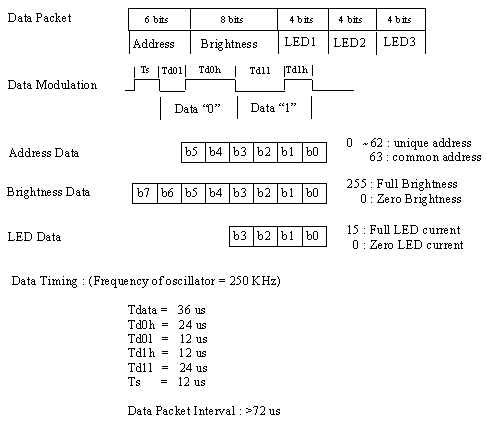
HL5225 is at default state when power on. Device address will be written in when first data packet is transferred into data input pin. The data packet includes 6 bits address data, 8 bits brightness data, 4 bits LED 1 current data, 4 bits LED 2 current data, and 4 bits LED 3 current data. When the address data in the following data packets is checked to be same as the address stored in HL5225, then the brightness data and 3 LED data will be written in HL5225, so the brightness of LED driven by HL5225 is controlled by input data.
The first bit of each data byte sent in to HL5225 is most-significant bit (MSB), and least-significant bit (LSB) is the last bit sent in to HL5225. The data bit in data packet must be modulated by Manchester coding scheme before being sent into HL5225. A low level signal with a duration of 1/3 bit duration time and follow a high level signal with a 2/3 bit duration time represent a logical low data bit. A low level signal with a duration of 2/3 bit duration time and follow a high level signal with a 1/3 bit duration time represent a logical high data bit. In each modulated data packet a high level signal with a 1/3 bit duration time must be put in the first place as start signal. There must have a separation time of at least 2 bit duration time insert in between the end and begin signal of two adjacent data packets.
The performance of brightness of LED driven by HL5225 is dependent on the brightness data and individual current data. The brightness data controls the pulse width of the current of LED drive. The minimum unit of pulse width is 1/255 full pulse width. A 0 value of brightness data will turn off the current of LED driver. The duration time of full pulse width is controlled by the internal oscillator. An external resister connected from ROSC pin of HL5225 to GND of power supply adjusts the frequency of internal oscillator of HL5225. The LED current data controls the current of LED driver. The maximum current level is 15. The step of current is 1/15 of maximum current of LED driver. A 0 value of LED current data will turn off the current of LED driver.
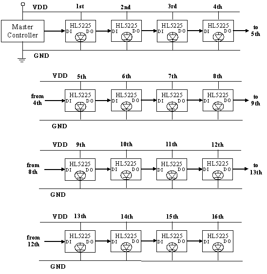
The data input and output pins of HL5225 can be cascade connected with the data input and output pins of the other HL5225 to form a daisy chain serial bus system. The address of each HL5225 connected in daisy chain serial bus system must be assigned after power on. The address data in first data packet is assigned to first HL5225 connected in the serial bus. The address data in second data packet is assigned to second HL5225 connected in the serial bus. The address data in third data packet is assigned to third HL5225 connected in the serial bus. The address data in following data packets is assigned one by one to the following HL5225 until the last HL5225 which are connected in the serial bus. The brightness data and LED current data will be written in HL5225 if the address data is match with the address data had been assigned to HL5225. The address data of number 63 is a common address. Only the brightness data of data packet with number 63 address data will be written in every HL5225 connected in the serial bus.
DATA FORMAT
PIN DESCRIPTION (HL5225A)
| PIN NO. | PIN NAME | I/O | FUNCTIONAL DESCRIPTION |
| 1 | LI1 | OUT | LED 1 Driver |
| 2 | GND | - | Ground of power supply |
| 3 | LI2 | OUT | LED 2 Driver |
| 4 | LI3 | OUT | LED 3 Driver |
| 5 | VDD | - | Positive power supply |
| 6 | DI | IN | Serial Data Input |
| 7 | DO | OUT | Serial Data Output |
| 8 | ROSC | I/O | Oscillator Resister |
APPLICATION CIRCUIT I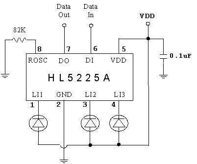
APPLICATION CIRCUIT II
Daisy Chain Connected Serial Bus System